
Knowledge
How does the capacitance of a passive probe affect signal transmission?
10:1 passive voltage probe is the core of hardware research and development, power electronic debugging commonly used accessories. Most engineers only pay attention to the nominal bandwidth of the probe, but ignore the key impact of various parasitic capacitances and compensation capacitors on signal transmission. Under low-frequency conditions, probe resistance dominates signal transmission; however, in high-frequency scenarios, capacitance is the core factor that determines waveform fidelity, which not only causes high-frequency signal attenuation and edge distortion, but also forms a capacitive load on the circuit under test, interfering with the original working state of the circuit, resulting in test distortion and misjudgment of circuit failure. This paper will briefly analyze the influence mechanism of probe capacitance and engineering optimization methods.
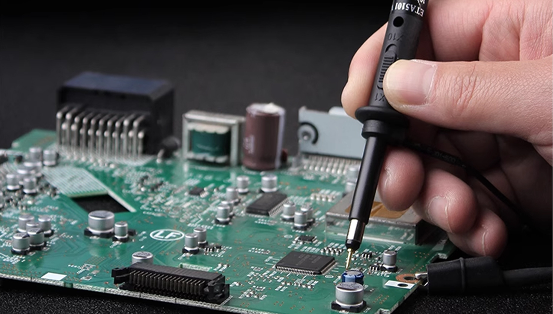
一、Primary source of capacitance for passive probe systems
The capacitance of the probe test system is composed of 4 parts in parallel, all of which are superimposed on the test node under test, which directly affects the transmission of high-frequency signals:
• tip parasitic capacitance cp:The stray capacitance formed by the probe metal and the shielding shell, with a value of 0.3~0.8pF, cannot be eliminated and is an inherent capacitive load of the test.
• Adjustable compensation capacitor Ccomp:The probe has a built-in fine-tuning capacitor (5 ~ 30pF), which is the only parameter that can be manually debugged for matching link tolerance and calibrating high-frequency response.
• Cable distributed capacitance Ccable:Coaxial cable core and shielding layer of the inherent distribution of capacitance, conventional parameters 8 ~ 10pF/ft, the longer the cable, the greater the total capacitance, the worse the high-frequency performance.
• Oscilloscope Input Capacitance Cscope:The front end of the oscilloscope is fixed to the ground capacitance (12 ~ 15pF), and the factory parameters are fixed and cannot be adjusted.
The core characteristics of capacitors are high-frequency low-capacitance reactance and low-frequency high-capacitance reactance, so there is almost no error in DC and low-frequency tests, while high-frequency signals will be seriously distorted due to capacitor shunt and bypass effects.
二、Distortion Mechanism of Capacitance to Probe Signal Transmission
1. Low-frequency ideal voltage divider, high-frequency capacitor-dominated transmission
Under low-frequency conditions, the 9MΩ series resistance of the probe and the 1MΩ input resistance of the oscilloscope form a standard 10:1 voltage division, and the signal has no distortion. After entering the MHz high-frequency band, the capacitive reactance is much smaller than the voltage-dividing resistor, the signal distribution is dominated by the capacitor instead of the resistor, and the high-frequency transmission accuracy depends entirely on the capacitance matching degree.
When the resistance voltage division ratio is accurately matched with the capacitance voltage division ratio, the full frequency band response of the probe is flat, and the high and low frequency signals are attenuated by 10 times. If the match is out of balance, there are two typical types of waveform defects:
• Undercompensation (small compensation capacitance):The capacitance is concentrated at the oscilloscope end, the high frequency component is greatly attenuated, the square wave edge becomes rounded, the rise time becomes longer, and the switching spike and ringing amplitude measurement are small.
• overcompensation (large compensation capacitance):The probe end capacitor is overloaded, the high frequency component is over-amplified, the waveform appears obvious overshoot, false ringing, easy to misjudge for circuit oscillation fault.
2. Total capacitance determines probe limit bandwidth
The combination of the probe and the oscilloscope can be equivalent to an RC low-pass filter. The larger the total capacitance of the system, the lower the-3dB bandwidth. The input capacitance of the 1:1 probe is as high as 60 ~ 100pF, and the bandwidth is only 6~10MHz; while the 10:1 probe can reduce the equivalent input capacitance to 10 ~ 15pF, and the bandwidth can reach 300~500MHz. Therefore, 10 × passive probes must be selected for high-frequency testing.
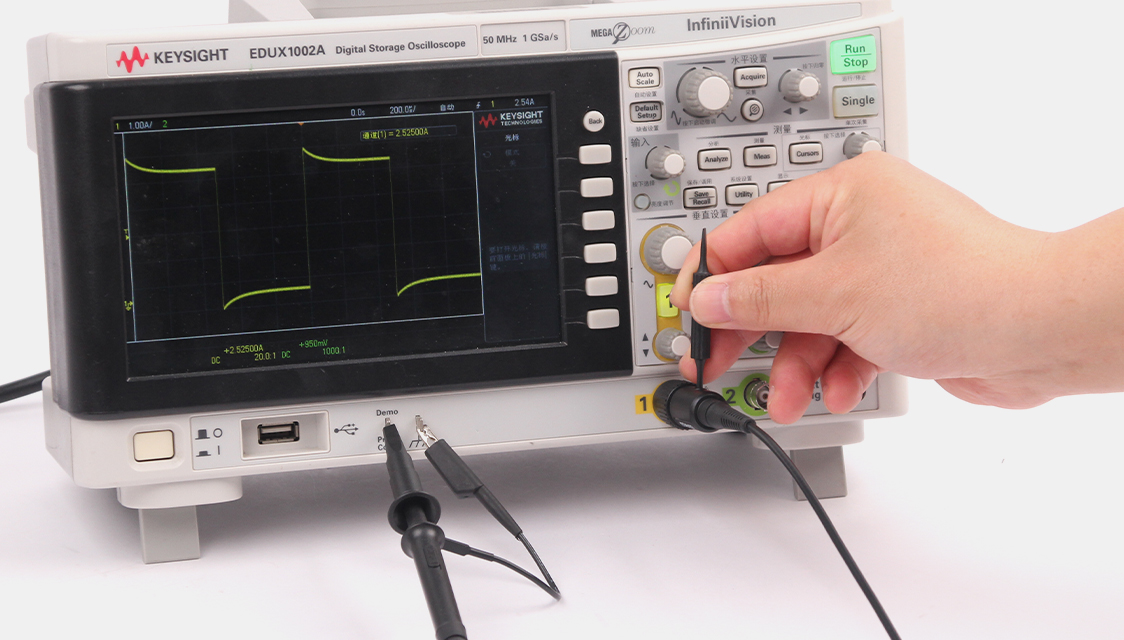
三、Load effect of probe capacitance: reverse interference with the circuit under test
Probe capacitance not only affects signal acquisition, but also changes the original circuit state of PCB as an external load, which is the core cause of high-frequency test distortion:
• Lengthen the signal edge to increase the switching loss error:In the MOS transistor gate, switching power supply and other high-impedance output nodes, the probe capacitance and the circuit output impedance form RC filtering, lengthening the rising edge of the signal. In SiC high-speed switching test, the rising edge is delayed by about 0.2ns for every 1pF probe capacitance increase, which directly leads to the deviation of switching loss calculation.
• Induced LC resonance, producing false ringing:PCB wiring, lead parasitic inductance and probe-to-ground capacitance form an LC resonant circuit. High-frequency switching signals will stimulate resonance, causing additional false ringing in the waveform and confusing the real circuit failure.
• Interfering with high-impedance nodes and changing circuit conditions:High impedance nodes such as voltage divider bias and operational amplifier input will change the static potential and RC time constant after the probe capacitance is connected in parallel, resulting in signal response lag, comparator flip delay, and interference with the normal working state of the circuit.
• Increased Miller effect, affecting device drive:When measuring the gate voltage of MOS and IGBT, the probe capacitance will increase the total capacitance value of the gate, extend the Miller platform, reduce the switching speed, and easily misjudge the lack of ability to drive the chip, resulting in heat generation and increased loss of the device.
四、Engineering practical operation optimization scheme to reduce capacitance test interference
1. Specification Probe Compensation Calibration
After replacing the probe and switching the oscilloscope channel, the compensation capacitor must be calibrated with the 1kHz standard square wave of the equipment to ensure that the waveform edge is straight, without overshoot and rounded corners, and to eliminate the system error caused by capacitance mismatch.
2. Minimize access capacitance
10:1 passive probe is preferred for high-frequency testing, and<1pF low-capacitance active probe is used for high-speed radio frequency and third-generation semiconductor testing. Remove the long grounding clamp and use the spring grounding pin to reduce the lead inductance. Simplify probe accessories and reduce parasitic capacitance at the tip.
3. Match probe model as required
Low-frequency power supply and high-impedance bias circuit are suitable for conventional 10:1 passive probe. SiC/GaN high-speed power circuit selects low-capacitance high-frequency probe. Resonance and radio frequency circuits shorten the test contact time, and use isolation probes when necessary to avoid changing the resonance characteristics of the circuit.
五、Summary
The resistance of the passive probe determines the low frequency attenuation multiple, and all kinds of capacitors directly determine the quality of high frequency signal transmission. Within the signal link, the capacitance matching degree affects the waveform transmission accuracy; at the end of the circuit under test, the parasitic capacitance will produce capacitive load interference and change the original signal characteristics. The effect of capacitance in low-speed test can be ignored, but in the high-frequency, high-speed third-generation semiconductor test scenario, the error caused by capacitance will be amplified sharply.
Engineers need to clarify the mechanism of probe capacitance, through standardized calibration, reasonable selection, optimization of testing methods, to avoid measurement distortion problems, to obtain true and accurate waveform data, to provide a reliable basis for circuit debugging and optimization.